
OXFORD, UK— For decades, silicon has reigned supreme in the solar energy market. But a new, unassuming class of crystal material called perovskite is rapidly emerging from research labs, threatening to upend the industry with its unprecedented efficiency and game-changing low-cost production potential. Dubbed a “wonder material” by researchers, perovskite is quickly rewriting the rules for how solar energy can be captured, promising to dramatically accelerate the global transition to clean power.
The Efficiency Revolution: Tandem Cells Break Records
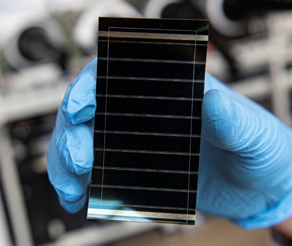
Perovskite’s greatest immediate impact is its ability to boost the output of conventional panels by forming a tandem solar cell. By stacking an ultra-thin perovskite layer on top of a standard silicon cell, researchers can capture a broader spectrum of sunlight, which neither material can do alone.
The results are staggering:
- Record Efficiency: The certified efficiency of perovskite-silicon tandem cells has soared, with a world record currently standing at 34.85%—comfortably surpassing the theoretical efficiency limit of a single-junction silicon cell (around 32%).
- Commercial Viability: Companies like Oxford PV have already demonstrated solar panels in an industrial format achieving a certified 25% efficiency, pushing commercial products well beyond the typical 21-23% for silicon modules.
The theoretical maximum efficiency for such a tandem cell is over 43%, suggesting there is still immense room for improvement.
The Lure of Low-Cost Manufacturing
What truly distinguishes perovskite from its silicon counterpart is its cost-effective manufacturing process. While silicon production requires high-energy, high-temperature fabrication in pristine cleanrooms, perovskite films can be solution-processed—essentially, painted, sprayed, or printed onto substrates at low temperatures.
This “ink-based” production method could drastically lower both the energy required to make the panels and the capital expenditure needed for manufacturing facilities. Furthermore, because the perovskite layer is incredibly thin—150 times thinner than a silicon wafer—it opens the door to revolutionary applications:
- Flexible and Transparent: Perovskite films can be applied to almost any surface, from car roofs and backpacks to mobile phone screens and, most significantly, the windows of skyscrapers to create “power-generating glass.”
- Widespread Accessibility: The low production cost promises to make solar energy cheaper and more accessible for consumers and utility-scale projects worldwide.
The Hurdles to Commercial Mainstream
Despite the dazzling lab results, perovskite has not yet replaced silicon on rooftops, primarily due to two major challenges:
- Stability and Longevity: This is the most critical hurdle. Perovskite materials are highly susceptible to degradation from moisture, heat, oxygen, and UV light. While conventional silicon panels are guaranteed to last 20–25 years, early perovskite cells failed in hours or days. Significant material engineering has improved projected lifespans to over 10 years in some pilot projects, but researchers must reliably reach the 25-year mark to compete for mass market adoption.
- Lead Toxicity: The most efficient perovskite formulations contain small amounts of lead. Although the amount is tiny compared to lead in coal-fired power production, concerns about potential environmental contamination and disposal must be addressed. Research is ongoing to develop non-lead or encapsulated alternatives to mitigate this risk.
The Race to ‘Fab’
The global race is now on to transition this lab-based marvel to a mass-manufacturing reality. Addressing stability and scalability will dictate the timeline for the solar revolution. If researchers can crack the durability code, perovskite will not just be another incremental improvement—it will be the disruptive technology that finally pushes solar energy past its current limits, defining the next generation of renewable power.