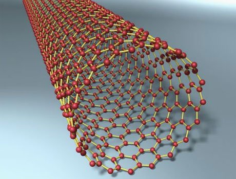
Scientists have demonstrated methods that could see higher-performance computer chips made from tiny straws of carbon called nanotubes.
Carbon nanotubes have long been known to have electronic properties superior to current silicon-based devices.
But difficulties in manipulating them have hampered nanotube-based chips.
The experiments, reported in Nature Nanotechnology, show a kind of two-part expoxy approach to individually place the nanotubes at high density.
The race is on in the semiconductor chip industry to replace current silicon technology – methods to make smaller and therefore faster devices will soon come up against physical limits on just how small a silicon device can be.
Study co-author James Hannon, a materials scientist at IBM, said that there are few realistic successors to silicon’s throne.
“The problem is you have to put it in to production on a 10- or 15-year time scale, so the kinks have to be worked out in the next few years,” he said.
“If you look at all the possibilities out there, there are very few that have actually produced an electronic device that would outperform silicon – there are exotic things out there but they’re all still at the <<PowerPoint stage>>.”
Though single nanotubes have shown vastly superior speed and energy characteristics in lab demonstrations, the challenge has been in so-called integration – getting billions of them placed onto a chip with the precision the industry now demands.
Current chips are made using lithography, in which large wafers of silicon are layered with other materials of different electronic properties and then devices are simply “etched” out using a focused beam of electrons or charged atoms.

To address the integration challenge, Dr. James Hannon and his colleagues came up with a solution – two of them in fact.
The first was a chemical that coats nanotubes and makes them soluble in water.
The second was a solution that binds to the first chemical and to the element hafnium, but not to silicon.
The team used standard techniques to etch a pattern of channels in hafnium deposited on silicon.
Then they simply “double-dipped” the chip into the two solutions – one chemical stuck to the hafnium, and the other chemical acted as the second part of a two-part epoxy, tightly binding nanotubes to the hafnium regions on the chip but not to silicon.
The result was a series of neatly aligned nanotube devices, already wired up within the pattern, at a density of a billion per square centimetre.
“That’s one nanotube every 150 or 200 (billionths of a metre) or so,” explained Dr. James Hannon.
“That’s not good enough to make a microprocessor yet – it’s a factor of 10 away.
“But it’s a factor of 100 better than has been done previously.”
The demonstration is a “huge improvement”, but Dr. James Hannon said several issues are still to be solved.
They include finding more efficient ways to sort through nanotubes – which are made in a wide variety of sizes and types – to select in large quantity and high accuracy the kind suitable for devices.
The etching process that sets the ultimate size of a transistor on the chip must also be improved.
For now, the team has modelled what it can do with the technique in its current form – a vast array of transistors, each comprising six nanotubes spaced 10 nanometres apart.
Their models suggest a 10-fold jump in performance – a chip run at more than three times the frequency and consuming just a third the energy.
However, in the longer term, nanotube chips would run up against the same limits that silicon faces; as Dr. James Hannon puts it, “we’re limited by the size of an atom eventually”.
“But this at least gives us a way to gain performance while shrinking the device.”